Remark:
1) The pin dimension of the product outline drawing is the size before tinning (it will become larger after tinning), and the mounting hole size is the recommended design size of the PCB board hole. The specific PCB board hole design size can be mapped and adjusted according to the actual producet.
2) In case of no tolerance shown in outline dimension:outline dimension ≤1mm,tolerance should be ±0.2mm;outline dimension> 1mm and≤5mm,tolerance should be±0.3mm;outline dimension>5mm,tolerance should be±0.4mm.
3) The tolerance without indicating for PCB layout is always±0.1mm.

Notes:
1) We recommend dust protected types for a clean environment(free from contaminations like H2S,SO2 or NO2 dust,ect.). We suggest to choose plastic sealed types and validate it in real application for an unclean environment(with contaminations like H2S,SO2 or NO2 dust,ect.)
2) Contact is recommended for suitable condition and specifications if water cleaning or surface process is involved in assembling relays on PCB.
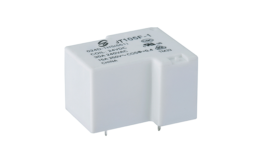
3) AgSnO2 contact can be represented as “(T)” after periodic code.
4) The customer special requirement express as special code after evaluating by JINTIAN.

 ENG
ENG
 contact number:0574-62502189
 Download
 position: